Many modern technologies, such as solar panels, cameras, biosensors and fiber optics, use photodetectors and sensors to transform light into electricity. Although these photodetectors have witnessed an overall increase in efficiency and decrease in cost lately, as they are becoming smaller, this reduction in size can also lead to problems concerning the efficiency of devices. Moreover, the chip manufacturing process poses its own set of problems: because the crystalline structure of the semiconductor film is directly aligned with the substrate wafer, transferring it to other substrate materials becomes difficult. Also, as mechanical exfoliation, where a piece of tape pulls off the semiconductor film and then transfers it to a new substrate, layer by layer, is used to transfer and stack these films, many non-uniform layers are stacked upon one another which leads to imperfections in the whole material. Finally, silicon, the mainly-used material for this process, performs worse, the thinner the material gets; alternative materials, on the other hand, also need a certain thickness to interact with light. Therefore, the main challenge is to produce thin, high quality photonic semiconductor films of materials other than silicon, to make the technology more efficient.
Now (2022), scientists at Penn State University’s School of Engineering and Applied Science created a new method of manufacturing atomically thin superlattices, or semiconductor films, which are highly light emissive.
Materials which are one atom thick generally take the shape of a lattice of geometrically aligned atoms that form a pattern specific to each material. A superlattice is a structure consisting of alternating layers of different materials which are typically measured in nanometers and therefore extremely small. They have completely new optical, chemical and physical properties which make them suitable for specific applications such as photo optics and other sensors.
The team at Penn Engineering engineered a superlattice which was five atoms thick and consisted of tungsten and sulfur (WS2). First, the scientists designed monolayers of atoms on a two-inch wafer and then dissolved the substrate, which made it possible to transfer the lattice to any desired material, in this case, a sapphire. Also, units of atoms were installed aligned in one direction to achieve a two-dimensional, compact and efficient superlattice. The scientists used a new type of structure in their superlattices which used exciton-polaritons, quasi-state particles made of half matter and half light. By manipulating the shape of the superlattice, they were able to indirectly control light emitted from it, which meant that the superlattice could be a light source.
For many years scientists have tried to harness the chemical properties of superlattices. In 2016, for example, scientists conducted chemiresistive and in situ GISAXS (grazing-incidence small-angle X-ray scattering) measurements simultaneously on superlattices which were self-assembled from 1-dodecanethiol (DDT)-stabilized gold nanoparticles. Treated with vapors (1000–10 000 ppm) of toluene, 4-methyl-2-pentanone and 1-propanol, the superlattice films showed reversible increases in both the interparticle distance and resistance. Additionally, the scientists also carried out a microgravimetrical analysis of the mass uptake due to analyte sorption. When they had a look at the partition coefficients, chemiresistive sensitivities and GISAXS-measured swelling for the three solvent vapours they discovered that they had the same trends, which were consistent with the solubility match between DDT and the analyte. The data for analyte sorption and swelling were also used to calculate the responses according to the commonly used chemiresistor model based on thermally activated charge transport. When they compared the calculated and measured responses they found that the model could predict the chemiresistive responses to the analytes only qualitatively.
Image: Experimental setup for in situ GISAXS/chemiresistor measurements. A custom made test chamber and substrates with defined areas for electrically addressing the GNP films and for positioning the X-ray spot were used to perform electrical measurements and GISAXS measurements simultaneously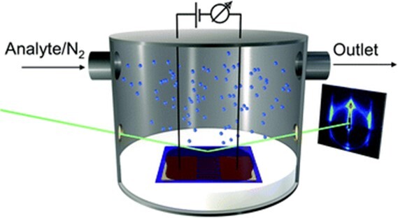
Source: Natalia Olichwer, Andreas Meyer, Mazlum Yesilmena, Tobias Vossmeyer* / Gold nanoparticle superlattices: correlating chemiresistive responses with analyte sorption and swelling†/ Journal of Materials Chemistry Issue 35, 2016/ doi.org/10.1039/C6TC02412B/ Open Access This article is licensed under a Creative Commons License CC BY-NC
In 2021, scientists analysed inhomogeneous moiré superlattices and using twisted-bilayer transition-metal dichalcogenides they showed how low-frequency Raman scattering could be used not only to detect atomic reconstruction, but also to describe the inhomogeneity of the moiré lattice over large areas as both the interlayer-breathing mode and moiré phonons were very susceptible to the moiré period and provided characteristic fingerprints. Hyperspectral Raman imaging visualised microscopic domains of a 5° twisted-bilayer sample with an effective twist-angle resolution of about 0.1°. They designed this method in order to allow for conveniently characterising and preselecting high-quality areas of samples for subsequent device fabrication, and for transport and optical experiments.
The new superlattice structures have several advantages: they can be made with a simple method that does not require multiple steps in a clean room, which enables the process to be repeated easily. Also, the design is applicable to many different types of materials. Being able to both emit and detect light with the same material will eventually lead to more complicated applications. One such technology that the superlattice could be used for is in integrated photonic computer chips which are powered by light. Other applications might include high-tech robotics, rockets, and lasers.
Image: Twist-angle dependence of low-frequency Raman scattering. a) Illustration of twisted-bilayer WSe2 in real space and the low-energy interlayer breathing mode with and without the presence of a moiré pattern. The green and orange lines sketch the landscape of the top and bottom layers. b) Low-frequency Raman spectra of bilayer WSe2 as a function of twist angle. The interlayer breathing modes are marked by asterisks and the dashed lines indicate the moiré phonon. The breathing mode (B) and shear mode (S) from the 2H natural bilayer (60°) are shown for reference. c) The twist-angle dependence of the breathing-mode frequency (red dots) clearly distinguishes three regimes of twist angles: atomic reconstruction (purple), where the breathing mode stiffens; large moiré unit cells (blue), where the breathing mode softens with increasing moiré period; and small moiré unit cells (yellow tint), where the breathing mode remains near constant with twist angle. The gray-dotted curve shows the twist-angle dependence of the moiré period. Errors from peak fitting are below the diameter of the spheres.
Source: Kai-Qiang Lin, Johannes Holler, Jonas M. Bauer, Philipp Parzefall, Marten Scheuck, Bo Peng, Tobias Korn, Sebastian Bange, John M. Lupton, Christian Schüller/ Large-Scale Mapping of Moiré Superlattices by Hyperspectral Raman Imaging/ Advanced Materials Volume 33, Issue 34 August 26, 2021/ doi.org/10.1002/adma.202008333/ Open Access This article is licensed under a Creative Commons License CC BY 4.0
Because of the wide range of applications for these superlattices, the scientists will, in a next step, be looking for means to adapt the scalability of the superlattices to different devices. If they succeed, we will soon be able to use faster computers as well as more efficient solar devices.
Solar Power
New Atomically Thin Material for Improved Light-Based Technology

Source: aenert.com