The idea to use sunlight for energy production is not new. The first modern solar cell was invented in 1954 at Bell Laboratories, an American industrial research and scientific development company now owned by Finnish company Nokia. Sunrays hitting the surface of a photovoltaic (PV) cell can be reflected, absorbed or pass through the solar cell. This is enabled by the semiconductor material of which the cell is composed. Semiconductors can conduct electricity better than an insulator but not as well as a good conductor like a metal. If the semiconductor is exposed to light, it absorbs the energy and transmits it to the negatively-charged electrons. This enables the electrons to flow through the material as an electrical current which is then transmitted to the grid through conductive metal contacts. The amount of electricity produced from PV cells depends on the intensity and wavelengths of the light available and multiple performance attributes of the cell. An important property of PV semiconductors is the bandgap, which indicates what wavelengths of light the material can absorb and convert to electrical energy. If the bandgap matches the wavelengths of the light hitting the PV cell, then the cell can efficiently make use of all the available energy.
Among the most-researched semiconductor materials are III-V compound semiconductors which are currently employed in space solar cells, concentrator solar cells, or in thermophotovoltaic generators. They are also suitable for multi-junction solar cells as they allow for different band gaps which are necessary to obtain efficiencies larger than 30%. Even though III-V cells are known for their high efficiency, their wider application has yet been hindered by the cost-intensity of the manufacturing process.
Now (2022), scientists at the U.S. Department of Energy’s National Renewable Energy Laboratory (NREL) have designed a solar cell showing a record 39.5% efficiency under 1-sun global illumination. This is the highest efficiency solar cell of any type, measured using standard 1-sun conditions.
Their work is based on earlier research performed in 2020 where they designed a solar cell with an efficiency of nearly 50%. This six-junction solar cell held the world record for the highest solar conversion efficiency at 47.1%, which was measured under concentrated illumination. Each of the six junctions of the cell was specially tuned to light frequencies from a specific part of the solar spectrum. The device consisted of about 140 total layers of various III-V materials to support the performance of these junctions.
The new solar cell is based on the well-known and thoroughly-tested inverted metamorphic multijunction (IMM) architecture that was invented at NREL. The improved efficiency was achieved by close study of research into quantum well solar cells, where many very thin layers are employed to modify solar cell properties. The scientists inserted the improved solar cell into a device with three junctions with different bandgaps. In order for the cells to be able to react to different parts of the solar spectrum, the scientists constructed them using III-V materials, such as gallium arsenide or aluminium arsenide, which span a wide range of energy bandgaps. Here, the top junction consisted of gallium indium phosphide (GaInP), the middle of gallium arsenide (GaAs) with quantum wells, and the bottom of lattice-mismatched gallium indium arsenide (GaInAs).
The scientists applied the quantum wells in the middle layer so as to extend the bandgap of the GaAs cell and increase the amount of light which can be absorbed by the cell. They also managed to develop very thin quantum well devices without major voltage loss. Moreover, they managed to anneal the GaInP top cell during the growth process to improve its performance, thus minimising the threading dislocation density in lattice-mismatched GaInAs. The efficiency of the new III-V cell was also tested for space applications, especially for communications satellites, usually powered by solar cells, and came in at 34.2% for a beginning-of-life measurement. The present design of the cell was found to be suitable for low-radiation environments. Higher-radiation applications might be enabled by further development of the cell structure.
Scientists have long sought to increase the efficiency of III-V solar cells. In 2018, scientists showed that in multi-quantum well solar cell devices consisting of gallium arsenide with bismuth (GaAsBi)/gallium arsenide under illumination hole-trapping was responsible for the reduced depletion width, an insulating region within a conductive, doped semiconductor material where the mobile charge carriers have been diffused away, or have been forced away by an electric field. Modelling of the quantum confinement energies in these devices demonstrated how the carrier escape times varied as functions of temperature, providing a tool for the design for future GaAsBi- based photovoltaic devices.
Image: Temperature dependent PL from QW20. The inset shows the temperature dependence of the estimated ground state transition (red points), along with a Varshni curve fitted to the data in the range 100 K-300 K (dotted line)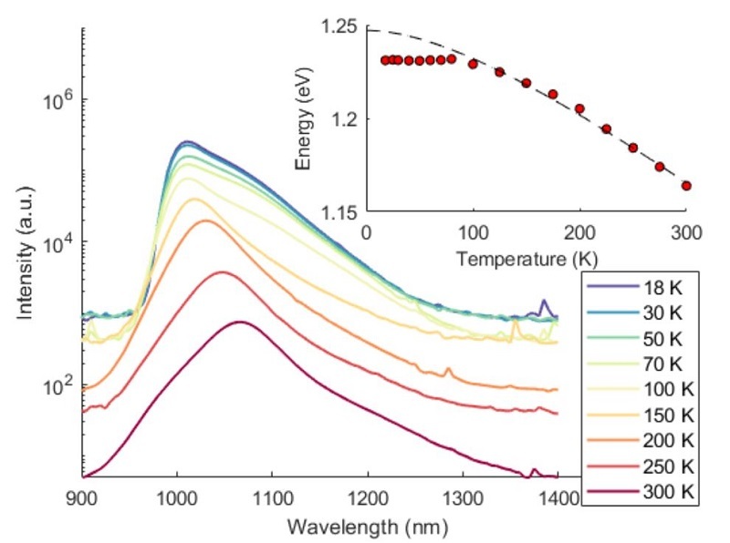
Source: Robert Douglas Richards, Mohamad Riduwan Nawawi, Thomas B. O. Rockett, Faezah Harun/ Light-biased IV characteristics of a GaAsBi/GaAs multiple quantum well pin diode at low temperature/ Semiconductor Science and Technology 33(9), July 2018/ DOI:10.1088/1361-6641/aad72a/ Open Source This article is licensed under a Creative Commons Attribution 3.0 Unported
In 2021, scientists designed lattice-matched GaAs-based solar cells especially using AlGaInP, AlGaAs, and GaInNAsSb materials, with the aim of achieving a wide spectral coverage spanning 0.7–2.2 eV. In order to further increase the efficiency toward 50%, they tested AlGaInP (>2 eV) and GaInNAsSb (<0.8 eV) subcells. AlGaInP cells with 0.1 Al composition were proved to show current-matching condition when built into a five-junction architecture together with two GaInNAsSb bottom and AlGaAs top junctions. Furthermore, current matching required for a six-junction tandem architecture was achieved for an Al composition of 0.26. The results of the research showed that fabrication of lattice-matched solar cells with more than four junctions was a realistic aim.
Image: Schematic structure of the LM 4J solar cell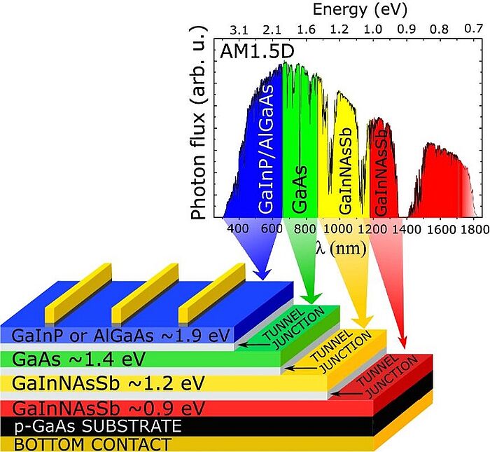
Source: Arto Aho, Riku Isoaho, Marianna Raappana, Timo Aho, Elina Anttola, Jari Lyytikäinen, Arttu Hietalahti, Ville Polojärvi, Antti Tukiainen, Jarno Reuna, Leo Peltomaa, Mircea Guina/ Wide spectral coverage (0.7–2.2 eV) lattice-matched multijunction solar cells based on AlGaInP, AlGaAs and GaInNAsSb materials/ Progress in Photovoltaics Volume29, Issue7 Special Issue: EU PVSEC, 9 Mar 2021/ doi.org/10.1002/pip.3412/ Open Source This article is licensed under a Creative Commons Attribution 4.0 International
The new cell constructed at NREL has many potential benefits: it is more efficient and has a simpler design that may be suitable for a variety of new applications, such as highly area-constrained applications or low-radiation space applications. However, even though gallium arsenide is generally used in III-V multijunction cells, it does not have the correct bandgap for a three-junction cell, which leads to unbalanced photocurrents between the three cells. Therefore, the bandgap was modified by using quantum wells. In this manner excellent material quality was preserved. Another aim of the research was to drastically reduce the manufacturing cost of III-V cells by providing alternate cell designs, which will make these cells economic for a variety of new applications.
The current research has the potential to open the door for the widespread application of III-V solar cells if the scientists indeed succeed in reducing manufacturing costs as well as making them available for a larger variety of applications. The prospects of achieving this goal are very promising.
Energy News Monitoring
New Solar Cell with an Efficiency of One Sun Developed