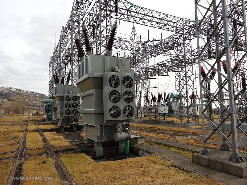
An electromagnetic pulse or EMP is caused by natural or artificial phenomena initiating a brief burst of electromagnetic energy. Among the most common events where this type of energy is released are solar flares or nuclear detonations. The electromagnetic energy of EMPs can be so forceful that communication systems are disrupted, electronic equipment gets damaged or even, on very rare occasions, buildings collapse. Electromagnetic pulses seldom occur, but if they do, they have the potential to incapacitate even the electric grid in a manner which would take a longer period of time to repair.
Now (2022), scientists at Sandia National Laboratories have designed an electronic device that is able to shunt excess electricity within an extremely short time and continue operation at a high voltage of 6,400 volts.
The basis of this device is formed by a diode. Diodes are electronic components allowing electricity to flow in only one direction through the device. One possible way of using them is to convert AC power into DC power, or in this case to divert potentially harmful high voltage away from sensitive grid transformers. The new EMP device by Sandia, however, uses the point at which the diode can no longer block the high voltage and shunts the excess current through itself to the ground and away from the grid equipment in a controlled manner. Another beneficial feature of the Sandia device is that it can quickly respond to fast voltage surges caused by EMPs.
The diode is made of gallium nitride, which is used, for example, in LEDs. Gallium nitride is a semiconductor which can hold off high amounts of voltage before it breaks down and is also able to quickly adapt to changes in the electric current. The scientists designed the diodes by engineering gallium nitride semiconductor layers using a process called chemical vapor deposition. For this purpose, they heated a commercially-available gallium nitride wafer to around 982 degrees Celsius and then added vapours containing gallium and nitrogen atoms. These chemicals formed layers of crystalline gallium nitride on the surface of the wafer. Using the so-called “baking” process, layers with different electrical properties could be produced which were then stacked upon one another in a specific order and further processed including etching and adding of electrical contacts.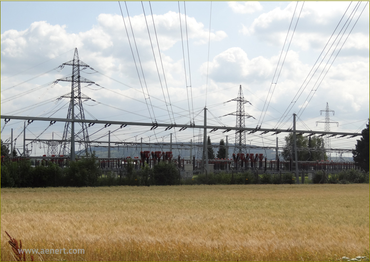
Once the device had been manufactured, tests were conducted on how it responded to induced fast voltage spikes which were similar to those occurring during an EMP. The challenge mainly consisted in modifying a tool to measure the extremely fast response time of the devices. Therefore, the team used very specialised equipment to apply a high voltage pulse and measure the electric pulse which was reflected back from the diode in order to find out when the device turned on.
A major challenge of building these very high voltage diodes was the necessity to create very thick gallium nitride layers which was difficult to achieve with commonly-used growth processes. A second major challenge was keeping the densities of crystalline defects, specifically impurities or missing atoms in the semiconductor material, very low throughout the growth time in order to generate devices that functioned well at very high voltages.
Scientists have long tried to make the electric grid more reliable in case of an emergency. In 2017, Van der Pauw structures, consisting of a four-point probe placed around the perimeter of the sample, on aluminium gallium nitride/gallium nitride high electron mobility transistors (HEMTs) with both silicon nitride and aluminium nitride passivation layers and both silicon carbide and gallium nitride substrates were designed in order to be able to study temperature dependent electron transport properties of two-dimensional electron gases (2DEG) in original and proton irradiated devices. They found that especially at low temperatures using a gallium nitride substrate or aluminium nitride passivation layer increased the mobility; however, this enhancement was greatly reduced upon irradiation with high proton fluences. The scientists assumed that the sheet density may be influenced by aluminium diffusion in the sample leading to electron donating impurities, which froze out around 200 K and were more visible in aluminium nitride passivated samples and minimised by using a gallium nitride over a silicon carbide substrate. Moreover, the experiment demonstrated that a large dose of radiation was responsible for the formation of traps in the aluminium gallium nitride layer, which decreased the sheet density at high proton fluences.
Image: Schematic of the three samples used in this study.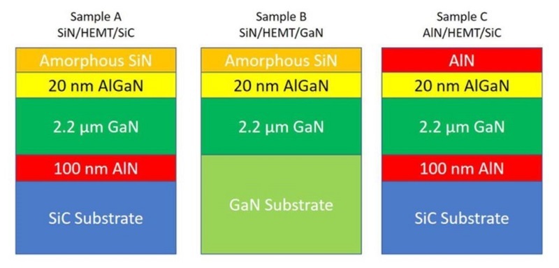
Source: J. C. Gallagher, T. J. Anderson, A. D. Koehler, N. A. Mahadik, A. Nath, B. D. Weaver, K. D. Hobart and F. J. Kub/ Effect of Surface Passivation and Substrate on Proton Irradiated AlGaN/GaN HEMT Transport Properties/ ECS Journal of Solid State Science and Technology, Volume 6, Number 11, 16 September 2017/ doi.org/10.1149/2.0151711jss/ Open Access This article is licensed under a Attribution 4.0 International (CC BY 4.0)
In 2022, scientists, including some who participated in the current research on EMP-dispersing devices, employed Raman spectroscopy to make out points of high crystal stress and non-uniform conductivity in a substrate. They also used optical profilometry to identify bumps and pits in a substrate which could cause severe device failures. The impact of the defects was analysed with the help of vertical P-i-N diodes with a single zone junction termination extension (JTE) edge termination and isolation, formed via nitrogen implantation. Electrical measurements yielded the result that the devices could continuously block voltages over 1000 V. The forward bias behaviour, on the other hand, was found to be able to consistently produce on-resistance below 2 mΩ cm2. The scientists also discovered that high crystal stress increased the probability of device failure from 6 to 20%. An inhomogeneous carrier concentration, meanwhile, had little effect on reverse bias behaviour, and slightly (~ 3%) increased the on-resistance (Ron). Optical profilometry was able to detect regions of high surface roughness, bumps, and pits. A large bump in the termination region of the JTE or a deep pit were found to be able to lead to a low voltage severe failure and increased crystal stress.
Image: Side view (a) and top view (b) diagrams of the vertical PN diodes fabricated for this study.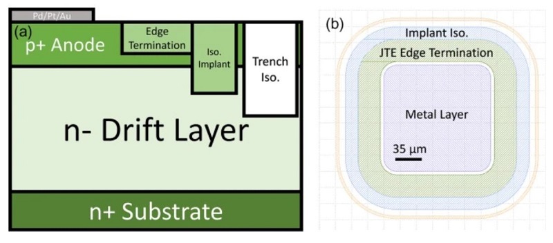
Source: James C. Gallagher, Mona A. Ebrish, Matthew A. Porter, Alan G. Jacobs, Brendan P. Gunning, Robert J. Kaplar, Karl D. Hobart & Travis J. Anderson/ Optimizing performance and yield of vertical GaN diodes using wafer scale optical techniques/ Scientific Reports volume 12, Article number: 658 (2022), 13 January 2022/ doi.org/10.1038/s41598-021-04170-2/ Open Access This article is licensed under a Attribution 4.0 International (CC BY 4.0)
The EMP device designed by Sandia scientists combines several advantageous features: apart from protecting the grid, diode devices like the gallium nitride diode can be used for many other purposes, including transformers for the grid, electronic devices to convert electricity from roof-top solar panels into power that can be used by household appliances, and even electric car charging infrastructure. Operating at higher voltage enables higher efficiencies and lower electricity losses. Also, diodes for these types of devices could easily be developed using existing infrastructure.
The final goal of the research is to achieve a device that operates at 20,000 volts, but this will require even thicker diode layers with fewer defects. If their research is successful, the scientists are confident that the device will one day make a valid contribution to providing modern society with reliable energy.
Energy News Monitoring
New electronic device to shunt excess electricity